

Light Guide Plate OEM Manufacturing Solutions for Precision Backlighting Needs
2026-11-20
Every backlight starts with a question most manufacturers don't ask until it's too late: how evenly will the light actually travel? At Meld Display, we treat the light guide plate not as a commodity, but as the quiet engine behind your display's brightness, uniformity, and power efficiency. In this post, we're breaking down what precision OEM manufacturing really looks like—from material selection and micro-structure design to the tolerances that separate a washed-out panel from a crisp, consistent glow. If your next product depends on backlighting that performs as precisely as it looks, you're in the right place.
Optical Patterns That Eliminate Hot Spots
Hot spots in an illuminated field rarely come from raw output alone. They emerge when periodic lenslet arrays or repeated prismatic features allow overlapping wavefronts to reinforce at regular intervals. Replacing that repetition with non-periodic micro-optic geometry breaks the alignment that creates bright patches, spreading energy into a smoother envelope rather than sharp local peaks.
A more direct route is to vary the local slope and curvature of each micro-structure by small, pseudo-random amounts while keeping the statistical distribution of angles fixed. This preserves the intended beam width but removes the faint grid-like coherence that many extruded or molded patterns leave behind. Because the eye is far more sensitive to contrast than to gradual change, even a few percent of randomization can make residual banding disappear.
Absorptive or high-scatter treatments are usually unnecessary once the pattern itself is decorrelated. The most reliable designs combine two or three uncorrelated structure depths, or offset rows by irrational fractions of the pitch, so no single spatial frequency dominates. The result is a field that still meets the same optical efficiency targets, but without the localized intensity spikes that read as hot spots.
Custom Microstructures for Slimmer Backlight Modules
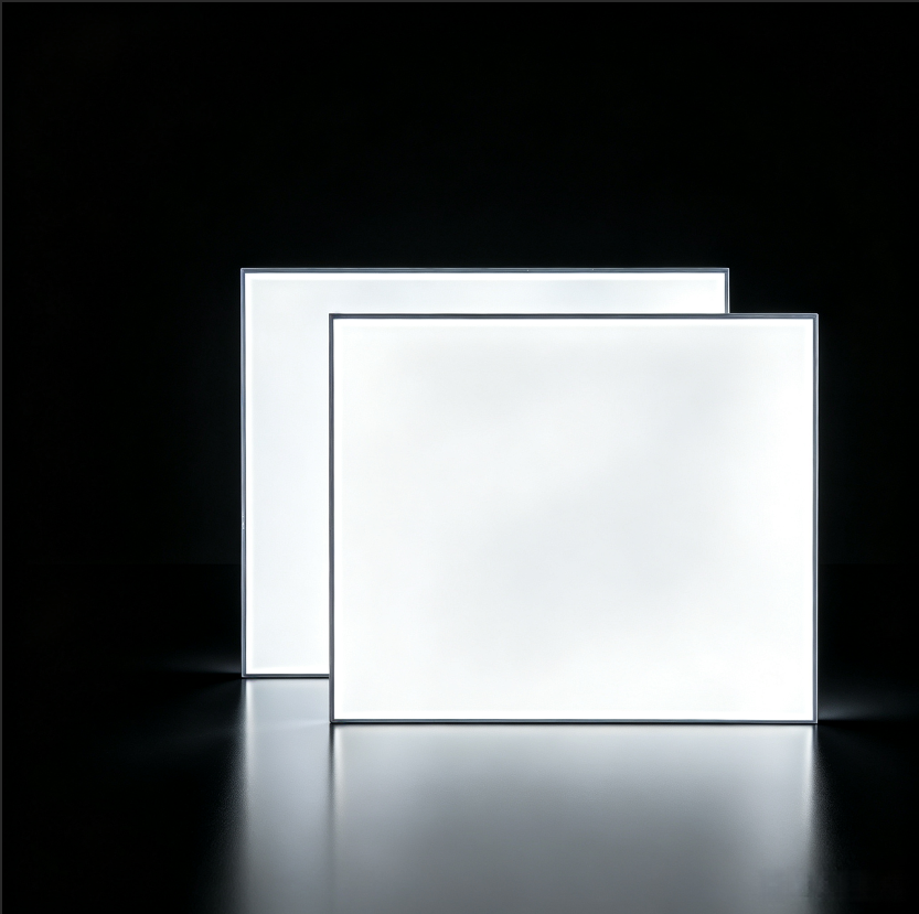
The push toward thinner displays rarely starts with the light source itself. Most design conversations jump straight to panel thickness or bezel width, while the backlight unit quietly consumes a fixed share of the stack. Custom microstructures flip that assumption. By etching or molding sub-millimeter patterns directly into the light guide plate, optical engineers can redirect light with far more precision than any flat diffuser allows. A few microns of geometric variation in a prism array can shift the exit angle enough to eliminate an entire layer of optical film, and that layer removal is where real slimness comes from.
What makes this approach interesting is how local the problem becomes. Instead of treating the whole module as one uniform system, designers tune microstructures for specific regions: finer pitches near the LED input edge to manage hotspotting, broader patterns toward the center to maintain uniformity without adding height. The patterns rarely look dramatic under a microscope, but their cumulative effect changes the mechanical envelope. Some recent edge-lit designs have dropped below three millimeters total thickness not by shrinking LEDs or using exotic materials, but simply by letting the light guide do more of the optical work that separate films used to handle.
The trade-off sits in the tooling. Once a custom pattern is cut into a mold, changing it means starting over, so prototypes tend to go through several quiet iterations before locking anything down. Yet for products where every fraction of a millimeter matters—wearables, automotive displays, foldables—that upfront effort pays back quickly. The result is a backlight that feels less like a stack of standardized parts and more like a component shaped around the product it lives in.
Prototype to High-Volume Production Without Losing Tolerance
Scaling from a handful of machined prototypes to thousands of parts per month usually exposes tolerances that were never really under control in the first place. A one-off can be finessed with extra setup time, hand finishing, or a sympathetic operator, but none of that survives contact with a production line. The first step is to identify which dimensions actually drive function and separate them from everything else that can float. Tight bands on non-critical features add cost without improving performance, while loose bands on critical interfaces guarantee field failures.
Once the critical tolerances are clear, the process itself needs to be treated as the source of dimensional truth. That means locking down fixture locating points, sequencing cuts or forming operations the same way every cycle, and recording offset adjustments rather than letting operators chase shifts by feel. Tool wear, thermal growth, and raw material variation from coil to coil or batch to batch tend to produce slow drifts that look random if nobody plots them over time. A short capability study at prototype volumes is often misleading; the real test is whether the process stays centered across multiple shifts, material lots, and tool changes.
Where the prototype process simply cannot hold the required band at rate, the answer is rarely to buy a better machine and hope for the best. Sometimes the tolerance can be transferred to a more stable feature or datum, or split across an assembly so no single part carries the full burden. In other cases, a deliberate in-process measurement loop makes more sense than trying to eliminate variation entirely. The goal is not to make every dimension perfect; it is to keep the few dimensions that matter inside limits while the line runs unattended, week after week.
Material Selection Based on End-Use Environment
The first and often most revealing filter in material selection is the environment where the product will actually live. A part that performs beautifully in a clean, temperature-controlled lab can fail within months on a coastal installation where salt spray, moisture, and intense sunlight work together. Rather than starting with a list of familiar grades, it helps to map out the specific exposure conditions: continuous immersion versus intermittent wetting, freeze-thaw cycles, UV intensity, airborne contaminants, and whether the material will sit idle or experience regular cleaning with solvents or abrasives.
Temperature and chemical compatibility deserve particular attention because their effects are rarely linear. A polymer that holds up well at room temperature may soften, oxidize, or lose impact strength when exposed to sustained heat, while metals can suffer from creep, scaling, or embrittlement at low temperatures. Chemical exposure is equally shape-shifting: dilute acids, alkaline cleaning agents, oils, and even oxygen can combine with temperature to accelerate degradation in ways that single-point data sheets do not capture. Matching the material to the full chemical profile of the operating environment, including transient exposures, prevents the kind of field failures that look puzzling in hindsight.
Once the environmental stressors are identified, the selection process becomes a narrowing exercise grounded in realistic constraints. Candidate materials should be screened for their stability under the most aggressive condition the part is likely to meet, not the average one. Prototype or coupon testing under actual service conditions, even for a short period, reveals interactions that catalog values miss, such as stress cracking around fittings, galvanic corrosion between dissimilar metals, or UV-induced discoloration that affects customer perception. This approach tends to produce fewer surprises later and leaves a clearer record of why a particular material was chosen over alternatives.
In-Line Optical Inspection Beyond Surface Defects
Most people still associate optical inspection with spotting scratches, pits, or contamination on a finished surface. That view misses a substantial part of what modern in-line systems actually deliver. The same cameras and lighting that flag a visible blemish can also verify edge geometry, hole presence, coating consistency, and subtle color shifts that indicate process drift. Once the system is positioned in the production line rather than at a final audit station, it stops being a simple defect filter and starts acting as a real-time window into process health.
The difference often comes down to how the image is acquired and interpreted. Multi-angle illumination, structured light, and high-speed line-scan sensors make it possible to catch issues that a single overhead photo would miss. A slight change in gloss, a micro-crack hidden by texture, or an adhesive bead that is continuous but too thin can all be measured without slowing the line. These are not exotic use cases; they show up in electronics, packaging, medical devices, and automotive assembly where cosmetic inspection alone is not enough.
What makes this shift practical is the feedback loop. Instead of sending a batch to the lab after production has moved on, operators see anomalies while they can still adjust a nozzle, a curing profile, or a material feed. That changes optical inspection from a gate that rejects defects into a tool that prevents them from recurring.
Collaborative Engineering From First Drawing to Final Assembly
A collaborative engineering effort really begins when the first sketch is still rough enough to argue over. Designers, machinists, and assembly leads gather around a marked-up drawing and talk through fit, material flow, and tool access before anything is locked in. It is not a formal review as much as a working session where the drawing absorbs practical knowledge from every side.
As the model matures, the same group keeps returning to the shared file with questions and redlines. A bracket moves because the assembly lead cannot reach a bolt. A bore diameter shifts after the machinist points out the closest available tool. These small decisions accumulate, and the drawing becomes less of a promise and more of a running agreement between disciplines.
By the time final assembly begins, most surprises have already been pulled out of the design. The drawings and the assembled machine line up because the people who touch the parts helped define them from the start. That continuity from first sketch to last bolt-torque is what turns a stack of drawings into a buildable design.
FAQ
Optical-grade PMMA and polycarbonate are the most common choices. The final call usually depends on thickness, thermal conditions, and whether the module needs extra stiffness or flame retardance.
Yes. We make plates for edge-lit modules where edge coupling efficiency matters, and for direct-lit designs where precise dot patterns or microstructures are needed to smooth out hot spots.
We run laser-based luminance mapping during the sampling stage and adjust dot density, depth, or lens geometry through iterative tooling corrections. For larger sizes, we generally check a 9-point grid on first articles before committing to production.
Laser-etched dots, micro-prism arrays, and custom textured finishes are all possible. The best pattern depends on LED pitch, mixing distance, and the viewing angle the backlight is designed for.
We often do. That can include optical simulation, material recommendations, and suggestions for reducing thickness or improving light coupling. A customer can send a rough backlight concept and we return a manufacturable plate design with measured samples.
We handle pilot builds starting in the low hundreds and scale up to high-volume programs. Tooling strategy shifts with quantity, so smaller batches may use a shared mold base while larger runs justify dedicated tooling.
Tooling is produced on precision engraving or lithography equipment, and process settings are logged for each cavity. Production plates are checked against a golden sample under a calibrated light source rather than relying only on visual inspection.
We inspect each batch for optical defects, dimensional accuracy, and luminance distribution. Flatness is checked under a gauge, and the active area is confirmed against the customer's mechanical drawing.
Conclusion
Precision backlighting starts with how light is distributed across the panel. In OEM manufacturing for light guide plates, hot spot control is treated as a geometric problem rather than an afterthought. Optical patterns are adjusted in density, depth, and angle across the surface so brightness stays even near LED inputs and at the panel edges. The same approach carries into slimmer backlight modules, where custom microstructures let designers reduce overall thickness without sacrificing luminance or widening tolerances. Those tolerances are held from prototype builds through high-volume runs because small shifts in feature geometry quickly show up as visible banding or dim corners. Material choice is matched to the end-use environment, whether the final assembly must handle heat, humidity, UV exposure, or repeated mechanical stress, so the light guide keeps performing outside a controlled test bench.
What separates a dependable OEM process from a basic fabrication service is how inspection and engineering are handled after the part leaves the mold. In-line optical checks look beyond scratches or contamination and evaluate the functional result, such as uniformity gradients and pattern registration, catching issues that surface-only inspection would miss. This becomes more useful when engineering support starts early. From the first drawing to final assembly, we work through LED placement, reflector gaps, adhesive zones, and mounting tolerances so the light guide fits into the broader backlight design instead of forcing the design around the part. The result is a manufacturing flow that keeps optical performance predictable and avoids the usual trial-and-error cycle when new backlight modules move from samples to full production.
Contact Us
Contact Person: Sky Wang
Email: [email protected]
Tel/WhatsApp: 8613430620125
Website: https://www.meldled.com/